
As the global semiconductor industry landscape undergoes profound transformation, a "core" battle for technological independence has begun on the northern bank of the Yangtze River.
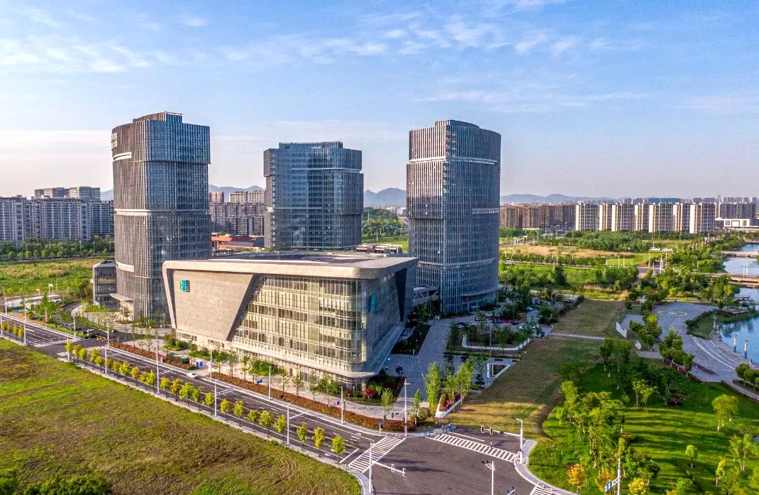
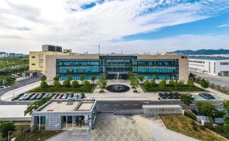
In September 2020, Jiangsu Xinde Semiconductor Technology Co., Ltd. (hereinafter referred to as "Xinde Semiconductor") was established in Nanjing Pukou Economic Development Zone. Within five years, this startup has achieved a remarkable turnaround from an industry newcomer to a Chinese unicorn. Today, with a strategic investment of 5.5 billion yuan, Xinde Semiconductor is fully committed to building an advanced packaging and testing base for artificial intelligence, launching an assault on the first tier of the global packaging and testing industry.
Marching forward with a focus on "innovation". Under the witness of the rolling Yangtze River, this rising "core" star will illuminate its new journey with the light of innovation and continue to write the era legend of the "Chinese core".
PART.01 A Southeast University English Major’s "Core" Breakthrough
In the vast galaxy of technological innovation, the semiconductor industry, with its sophisticated processes and profound technologies, has built professional barriers that are hard for ordinary people to cross. Therefore, few entrants with a liberal arts background can stand out in this field. However, Zhang Guodong, the leader of Xinde Semiconductor, has made his mark in the chip packaging field through a magnificent cross-border counterattack.
In the midsummer of 2001, Zhang Guodong stepped into society with a graduation certificate in English from Southeast University. At that time, although China would not officially open the door to the WTO until December of that year, the spring breeze of the foreign trade industry had already swept across the land of China. While his classmates chose traditional paths such as translation and education, this young man made an unexpected decision: to join an integrated circuit technology enterprise and become a customer engineer.
Zhang Guodong was well aware that in the technology-intensive field of integrated circuit manufacturing, language is merely a bridge for communication, and the real value lies in whether one can become a "bilingual speaker" of technology and business. To gain an in-depth understanding of the technical logic and manufacturing processes behind the products, he took the initiative to dive into the technical department. He not only observed every production detail with his eyes but also carefully recorded every technical point in his mind. This seemingly accidental technical enlightenment actually laid a key groundwork for his cross-border development in the future.
In 2003, Zhang Guodong moved to a semiconductor enterprise focusing on advanced packaging technology. 95% of this enterprise’s customers were from semiconductor powerhouses such as Europe and the United States, and each order was a direct dialogue with international giants. He grew rapidly under the dual tempering of technology and the market. He not only transformed from a customer engineer to a technical expert but also unconsciously weaved a network of contacts covering the global semiconductor industrial chain.
In 2021, after deeply engaging in the industry for 20 years, Zhang Guodong keenly noticed that against the backdrop of Moore’s Law gradually losing its effect, advanced packaging technology was becoming a key path to continue the improvement of chip performance, yet there was still a generational gap between China and the international leading level in this field. With the ambition of "rising suddenly in the independent track of advanced packaging and becoming an industry benchmark" to serve the country through industrial development, he resolutely took up the banner of entrepreneurship, joined Xinde Semiconductor, and became the leader of this enterprise.
The road to entrepreneurship is never smooth. When Xinde Semiconductor was first established, it coincided with a special period, and challenges such as supply chain disruptions and logistics difficulties came one after another. Nevertheless, it was in such adverse circumstances that Zhang Guodong led the entrepreneurial team to create the remarkable "Xinde Speed" in the industry—quickly completing the completion and commissioning of the first project and significantly shortening the average construction cycle of the industry.
"Once the bow is drawn, there is no turning back. We can only rely on the team’s profound technical accumulation and efficient execution to blaze trails through mountains, build bridges over waters, and overcome obstacles all the way," said Fang Yaping, General Assistant of the Secretary Office of Xinde Semiconductor.
PART.02 The "Core" Force That Became a Unicorn in Three Years
In the grand landscape of the global semiconductor industry, chip packaging and testing is an extremely critical downstream link, and the importance of packaging and testing enterprises is self-evident. Amid this fierce competition filled with industry leaders, Xinde Semiconductor—established for less than five years—has emerged as a dark horse, achieving simultaneous breakthroughs in three dimensions: technology R&D, market development, and capital operation, and creating an industry miracle of being listed on Forbes China’s New Unicorn List within three years.
"Since its establishment, the company has targeted the commanding heights of advanced packaging technology. By building a complete mid-to-high-end packaging technology matrix, our products have deeply penetrated core application scenarios such as consumer electronics, 5G communications, and the Internet of Things (IoT)," Fang Yaping stated. Behind these words lies the countless days and nights of efforts by Xinde Semiconductor’s R&D team to overcome challenges.
In June 2022, Xinde Semiconductor Advanced Packaging Technology Research Institute was officially established, and Dr. Hu Chuan—a national distinguished expert and academic leader of the Semiconductor Research Institute of Guangdong Academy of Sciences—was invited to serve as its first dean. This strategic layout soon yielded results: in March of the following year, the research institute launched the landmark CAPiC Die and Advanced Packaging Technology Platform.
At the same time, Xinde Semiconductor has leveraged Nanjing’s rich scientific and educational resources, establishing in-depth strategic partnerships with integrated circuit schools of universities such as Nanjing University of Posts and Telecommunications and Nanjing University of Information Science & Technology. This integrated "industry-academia-research-application" innovation model has not only accelerated the transformation of technological achievements but also promoted positive interaction between the industrial chain and the innovation chain.
Currently, Xinde Semiconductor has successfully overcome a number of "chokepoint" challenges and built a complete technology matrix: it has achieved large-scale mass production of mainstream packaging technologies such as BGA (Ball Grid Array), LGA (Land Grid Array), and CSP (Chip Scale Package); it holds significant competitive advantages in advanced process fields including Bumping (wafer bumping), Fan-out (fan-out packaging), FC (Flip Chip), and SiP (System in Package), firmly ranking among the first tier of China’s packaging and testing industry. Looking to the future, the company is actively deploying cutting-edge technologies such as glass substrate embedding, 2.5D glass interposers, and Hybrid Bonding, continuously consolidating its technological leadership in the high-end packaging and testing field.
Since its establishment, this emerging technology enterprise has successfully raised over 2 billion yuan in development funds, with an impressive list of investors: it includes not only professional investment institutions such as Nanjing Venture Capital Group, Shenzhen Venture Capital, and Jinpu Fund but also industrial giants like MediaTek, Xiaomi, and OPPO.
Fang Yaping revealed that in the semiconductor packaging and testing industry, the customer onboarding cycle is quite long. The entire process—from initial contact to end-product verification, small-batch trial production, and large-scale mass production—often takes more than a year. However, it is this "long-distance race" that allows customers to comprehensively evaluate Xinde Semiconductor’s technical capabilities and management standards. First, customers verify the technology through orders; then, they "vote" for the future with real investment. In this ecosystem, Xinde Semiconductor is not only an innovator of technology but also a connector of value, demonstrating a growth dimension far beyond that of traditional packaging and testing enterprises.
PART.03 The "Core" Landmark Rising on the Northern Bank of the Yangtze River
Driven by the strong momentum of popular applications such as artificial intelligence (AI), high-performance computing, and automotive intelligence, China’s packaging and testing industry has ushered in a new wave of capacity expansion since the beginning of this year. Leading enterprises have successively increased investment in advanced packaging capacity construction, driving the industry to transform and upgrade toward higher technology content and higher added value.
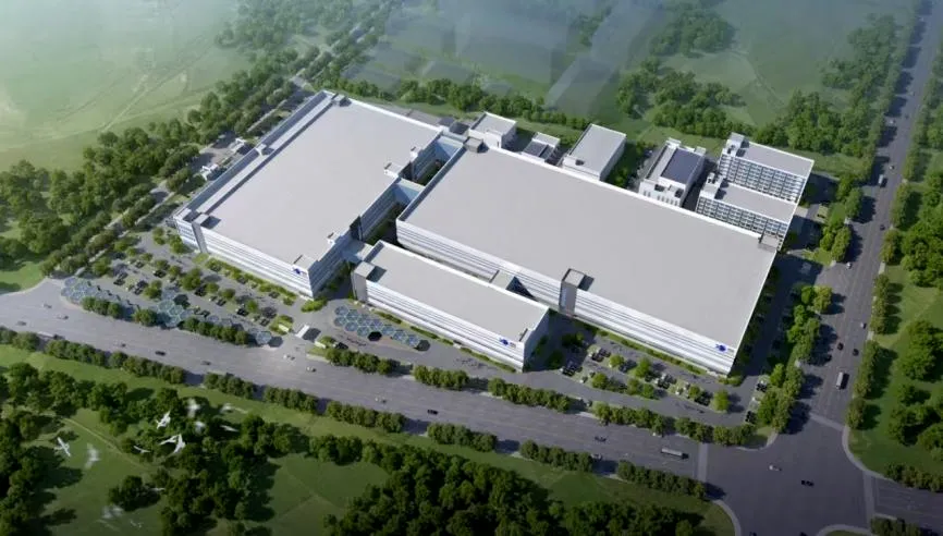
On June 30, the project of Xinde Semiconductor’s AI Advanced Packaging and Testing Base officially broke ground, with a total investment of 5.5 billion yuan. Among this, the first phase will involve an investment of 1 billion yuan, with plans to construct 153,000 square meters of modern workshops and build two world-leading high-end packaging production lines. The project will fully tackle the challenges in AI computing chip packaging and accurately meet the high-performance packaging needs of 5G communications and automotive-grade chips.
A relevant person in charge of the 5th Investment Department of Nanjing Venture Capital Group stated that as a key target in the construction of Nanjing's integrated circuit industry ecosystem, the core investment value of Xinde Semiconductor Technology lies in the in-depth alignment between its technological strategic significance and the needs of regional industrial upgrading. Nanjing's "4266" modern industrial system clearly identifies integrated circuits as a core track, and the advanced packaging capacity such as 2.5D Chiplet deployed by Xinde Semiconductor is resonating with the strategic direction of building an industrial cluster with global influence in the region.
The person in charge further pointed out that Jiangsu Province accounts for 31% of the national integrated circuit output value, but there is an industrial gradient gap between Nanjing and major packaging and testing cities such as Wuxi. As a scarce local advanced packaging enterprise, Xinde Semiconductor's capacity expansion can effectively make up for Nanjing's shortcomings in the semiconductor manufacturing link. "The company's core team has industrialization experience in leading enterprises. In 2024, the company's revenue grew by 57.72%, significantly higher than the industry average, which fully demonstrates its commercialization capability," the person in charge added.
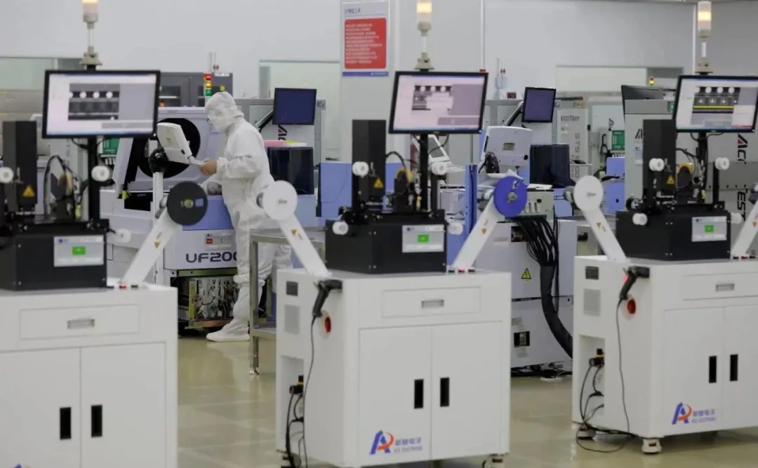
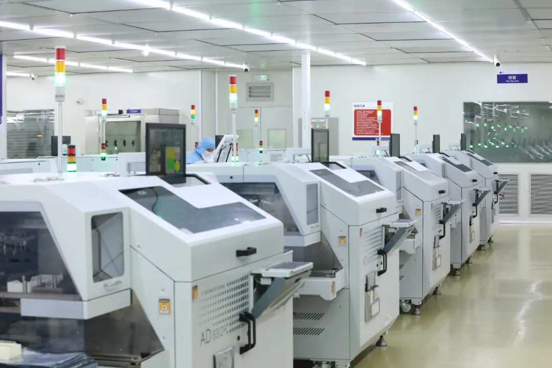
Walking into the three-story factory area of Xinde Semiconductor, dicing saws are cutting with micron-level precision, wire bonders are threading like skilled embroiderers, and wafer-level packaging lithography machines worth tens of millions of yuan are leading the micron-level precision processing... More than 2,000 such high-precision devices have built the company's heavy asset barrier of over 2.7 billion yuan. They are not only "giants" that consume capital but also "furnaces" that nurture innovation, confirming the survival rule of the semiconductor industry of "exchanging capital density for technological height".
It is reported that Nanjing Industrial Fund has provided targeted support to Xinde Semiconductor. By adopting a "point-to-area" approach, it has strengthened the magnetic attraction effect of the regional packaging and testing industry cluster, while leveraging the enterprise’s heavy-asset attribute to build a more solid foundation for the industrial ecosystem. Focusing on long-term development, the company completed its shareholding system reform on June 27, 2024, and plans to officially enter the capital market by 2028.
Xinde Semiconductor’s take-off trajectory is like a prism, reflecting the vigorous vitality of the integrated circuit industry in Pukou Economic Development Zone. With the company as the center, major enterprises such as TSMC, King Yuan Electronics, and Huatian Technology have gathered within a 5-kilometer radius, forming a complete industrial closed loop covering raw material supply, equipment maintenance, and end-user applications. "Here, many of our suppliers, partners, and customers are close at hand, and this industrial collaboration efficiency is unmatched by other regions," Fang Yaping said with emotion.
On this "core" field that nurtures hope, the industrial achievements are abundant: in 2024, the integrated circuit industry in Pukou District achieved a revenue of 26.5 billion yuan, with a year-on-year growth of 15.4%, and its industrial scale has maintained the first place in the city. As major projects such as Xinde Semiconductor and Huatian Technology are put into production one after another, this "core" landmark rising on the northern bank of the Yangtze River will surely shine more brilliantly and illuminate a new landscape for China’s semiconductor industry.
Source: Venture Capital Group
Review: Xue Yao
Release: You Yi