
On the microscopic battlefield of semiconductor manufacturing, a precision campaign determining the fate of "China's chips" has quietly commenced. Here, as chip processes advance into the nanoscale, cleaning technology faces the ultimate challenge of "accurately removing a single strand of hair on a football field."
In this critical field of semiconductor cleaning, Jiangsu Flat Semiconductor Equipment Co., Ltd. (hereinafter referred to as "Flat") has evolved from an obscure startup into one of the few domestic enterprises capable of providing 19nm-level wet cleaning equipment, successfully breaching the technological defenses long guarded by foreign companies.
Flat's growth trajectory has become a vivid case study in the observation of China's semiconductor equipment localization efforts.

Breaking Through the Trust Barrier: From "Bench Player" to "Star Performer"
In 2004, Zhong Lihua, fresh out of university, stepped into the doors of a Nanjing-based joint venture specializing in liquid crystal display technology. Over the following years, though he moved between several companies, he remained deeply rooted in the semiconductor display industry, witnessing every technological leap firsthand. "For me, once I stepped into this field, it became a lifelong commitment," Zhong Lihua recalled with a smile.
Over a decade, he worked day in and day out with semiconductor display production line equipment such as cleaning, etching, and photoresist removal, accumulating extensive technical and management experience. Yet, one harsh reality always stung him: the domestic semiconductor equipment market was largely dominated by foreign companies, particularly those from Japan and South Korea, which held the vast majority of market share.
In 2013, an idea sparked in his mind: "Since we’ve mastered these technologies, why not start our own venture?" Zhong Lihua and his team decided to focus on wet etching technology in panel manufacturing, collaborating with Nanjing University of Science and Technologyform a breakthrough research team. They worked tirelessly, debugging and optimizing their systems day and night.Two years later, they delivered an inspiring result: the team developed China’s first etching solution concentration management system, achieving a comprehensive breakthrough in real-time monitoring, intelligent analysis, and precise control of chemical concentrations.
However, the question of "who to sell it to" encountered unexpected challenges. While imported products with similar performance sold for over RMB 2 million, the company’s offering was priced at just half of that. Despite its competitive pricing, customers remained hesitant: "Saving RMB 1 million on price is one thing, but if your product isn’t reliable, it could lead to mass production line failures, causing losses of millions or even tens of millions." In the face of such high stakes, price advantages seemed trivial.
To address this, the team took their equipment directly to customer factories for live testing. Although all performance metrics met standards, customers scrutinized it repeatedly but still hesitated to place orders. This was the most difficult bottleneck in the localization of process equipment—the trust barrier. When reliability had yet to be proven in the market, every potential customer adopted a wait-and-see approach.
A turning point came unexpectedly. When a piece of equipment at a Nanjing-based company suddenly malfunctioned, the imported equipment manufacturer’s after-sales service was sluggish, and the issue remained unresolved for far too long. Switching to another foreign brand meant facing delivery times of up to six months, which the company simply couldn’t afford.
"Delivery within two months, with guaranteed quality!" Zhong Lihua seized the opportunity to make a bold pledge, and the customer agreed, albeit skeptically. In the end, the team not only delivered on time but also exceeded the customer’s expectations with the equipment’s performance.
Word of mouth began to spread like ripples. Initially, customers remained cautious: "For an order of 20 units, we’ll try two from you first." The team persevered, "tackling one unit at a time, grinding out one order at a time," gradually pushing their etching solution concentration management system to the top of the industry sales charts. They had transformed from a "bench player" on the production line to a "star performer."
Breaking Technological Barriers: The "Ultimate Challenge" on the Nanoscale Battlefield
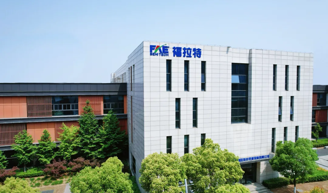
Today, at Flat’s facility located in Hongfeng Science Park, Qixia District, employees are frequently seen pushing logistics carts laden with equipment, busy shipping these precision instruments to every corner of the country.
In fact, having keenly observed the surging demand for the localization of wet cleaning equipment, Zhong Lihua had already made a strategic pivot, leading his team to expand their core business: evolving from a supplier of key chemical concentration detection and management systems for wet process equipment into a comprehensive one-stop solution provider for semiconductor wet processes.
Amid the global tech competition landscape, the semiconductor industry holds a particularly prominent position, with chip manufacturing at its core. Semiconductor cleaning acts as a "health guardian" for chip production, effectively preventing impurities from compromising chip yield and product performance.
On one hand, current chip manufacturing processes incorporate wet processing steps before and after repetitive stages such as lithography, etching, and deposition. These wet steps account for over 30% of the entire chip manufacturing process, making them the most extensive segment. On the other hand, as the circuit line widths of modern chips have shrunk to the nanoscale and structural complexity continues to increase, sensitivity to impurities has correspondingly intensified. Semiconductor cleaning is now evolving toward greater precision and specialization.
Take smartphone chips as an example: a single chip undergoes hundreds of cleaning cycles during manufacturing—much like thoroughly cleaning the work surface after each layer of a mille-feuille cake is added (each layer representing a deposited circuit). A single pixel on a smartphone display measures just about 20 micrometers, roughly one-quarter the diameter of a human hair, and a single chip integrates hundreds of millions of such intricate structures. "Imagine pinpointing and removing ultrafine particulate contaminants across an area the size of a standard football field—that’s the level of difficulty semiconductor cleaning entails," Zhong Lihua explained.
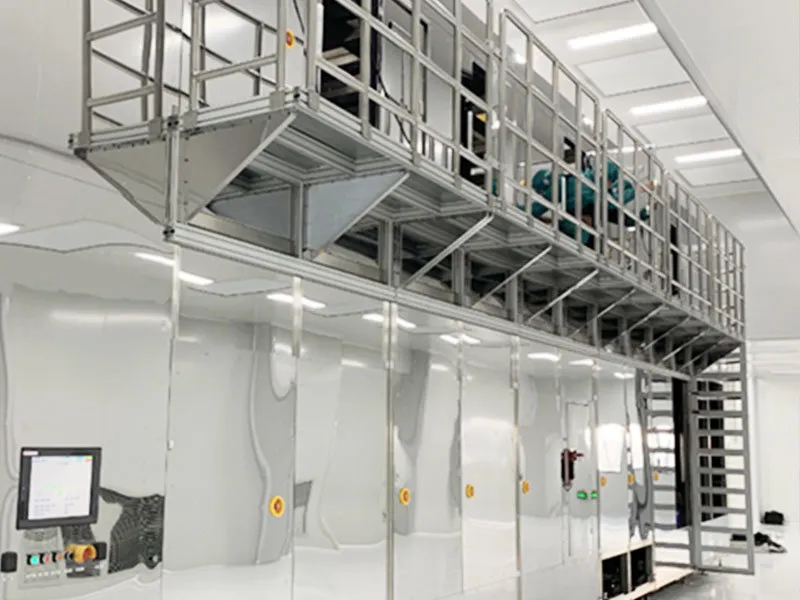
Wet cleaning is the mainstream technical approach in semiconductor cleaning. Depending on specific process requirements, it employs specialized chemical solutions and deionized water, combined with auxiliary methods such as ultrasonic oscillation and vacuum suction, to remove particles, natural oxide layers, organic residues, metal contaminants, and other impurities during wafer manufacturing—all while ensuring zero damage to the substrate.
Today, Flat has not only successfully developed core wet process equipment, including single-wafer and batch wet cleaning systems, but has also delivered mass-production-ready machines. These advancements have helped customers across multiple sectors break through technical bottlenecks, gain market advantages, and challenge the dominance of foreign monopolies. As a result, Flat has been recognized as a "Top Supplier" by several leading clients.
Notably, Flat’s independently developed single-wafer wet cleaning equipment has advanced process nodes to 19nm, placing it at the forefront of domestic capabilities. Behind this breakthrough lie countless scrapped test wafers, endless adjustments to process parameters, and innumerable sleepless nights.
"Every incremental advancement in wet equipment specifications is an ultimate challenge," Zhong Lihua reflected.
Industry Transformation: Seizing the High Ground in Advanced Display Technology
In May of this year, Flat officially announced the completion of a tens of millions of yuan Pre-A round financing. This round was jointly invested by Nanjing Venture Capital Group, Xingang High-Tech Investment, and Oriental Capital, fully demonstrating the capital market's recognition of the company.
Hu Yong, General Manager of Investment Department V at Nanjing Venture Capital Group, stated: "Flat has not only achieved technological breakthroughs but also built a complete ecosystem covering equipment R&D, production, and after-sales services. This comprehensive capability is exactly what we value."
It is reported that after completing this round of financing, the company has officially changed its name from "Jiangsu Flat Automation Equipment Co., Ltd." to "Jiangsu Flat Semiconductor Equipment Co., Ltd.", marking a comprehensive upgrade of its business landscape.
Looking forward, Flat will focus on four key directions: first, concentrating on high-end semiconductor wet process equipment and developing core equipment for next-generation semiconductor display technologies; second, expanding production bases to enhance large-scale delivery capabilities; third, deepening strategic partnerships with leading companies in various semiconductor sectors such as micro-displays, logic circuits, and power devices; and fourth, establishing innovation consortiums with institutions like Shanghai Jiao Tong University, Nanjing University of Science and Technology, Nanjing Tech University, and Nanjing Forestry University to create a closed loop from "technology R&D - pilot testing - industrialization".
Focusing on the development of core equipment for next-generation semiconductor display technologies is undoubtedly the most strategic move. As emerging display technologies such as OLED, Mini LED, Micro LED, and Micro OLED complete the transition from laboratory research to production lines, the entire industry stands on the brink of explosive growth. Market research data indicates that by 2027, global investment in the new display industry will exceed 1.5 trillion yuan, with the wet process equipment market alone expected to reach 20 billion yuan.
In this wave of display technology upgrades, domestic equipment manufacturers are for the first time standing on the same starting line as international giants. "This is our historic opportunity to shift from following to leading," revealed Zhong Lihua. Flat is currently making inroads into core segments such as AR, VR, and AI glasses—fields that are at the tipping point of technological breakthrough and commercial explosion.
With 20 years of deep experience in the semiconductor display industry, Zhong Lihua understands well that in the field of high-end manufacturing, markets are never "taken" but are earned inch by inch. When Chinese companies truly master core technologies, the global industrial landscape will inevitably be reshaped.
Source: Venture Capital Group
Reviewed by: Xue Yao
Published by: You Yi